Innovating Through Precision and Speed: How Laser Etching Is Redefining RF Manufacturing
As satellites shrink, 5G systems scale, and sensing technologies push into harsher and more demanding environments, the margin for error all but disappears. Circuit traces must be tighter. Performance must be repeatable. And manufacturing processes must keep pace with an industry that no longer has time to slow down.
This is where the story of laser etching begins, not as a replacement for what came before, but as a smarter, faster way forward.

The Foundation: Gold Circuits Built for Reliability
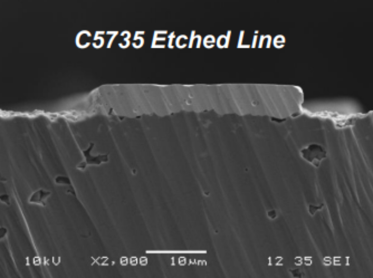
For decades, gold hybrid circuits have been trusted in RF applications where stability is non-negotiable. Thick film gold metallizations such as C5735 offer corrosion resistance, dense microstructures, and excellent electrical performance, critical attributes when even the slightest variation can disrupt impedance or increase signal loss.
Etching has long been the method of choice to shape these materials into precise, compact circuit geometries. High-reliability testing shows etched gold circuitry maintains electrical integrity and wire bondability, even under rigorous thermal aging and cycling.
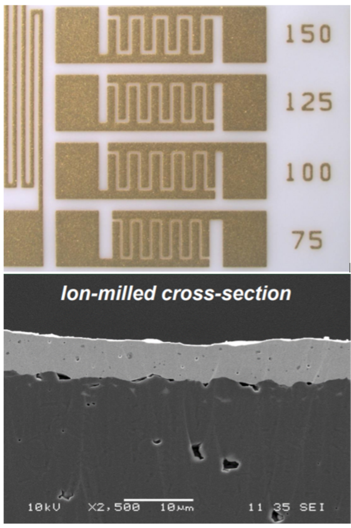
As RF designs continue to advance, the demands on circuit patterning increase. Fine conductor widths, precise spacing, and consistent edge definition are essential for maintaining signal integrity and repeatable performance. Modern etching processes consistently deliver precise geometries for both prototyping and high-volume production.
As designs become more compact, etching is no longer optional. it’s essential. But how that etching is done makes all the difference.
The Traditional Path: Proven, but Process-Heavy
Chemical etching is a proven, reliable process for mid-volume production. Using photoresist imaging and wet etching, manufacturers can achieve finer trace widths than screen printing alone.
Its strengths are well known:
- Uniform, well-defined circuit lines
- Scalability for mid-volume manufacturing
- Familiarity across the industry
.png)
Yet, behind the scenes, chemical etching brings complexity.
Multiple processing steps add time at every stage. Strong oxidizers and complexing agents are required to remove dense gold films. Solutions like HNO₃/HCl, KI/I₂, or even sodium or potassium cyanide must be carefully managed, each with its own etch rate, disposal requirements, and environmental, health, and safety considerations.
Managing these hazards doesn’t just require compliance; it requires infrastructure, training, strict PPE protocols, and emergency preparedness. All of it adds cost, slows iteration, and introduces risk outside the circuit itself.
As RF development cycles continue to compress, the question becomes clear: Is there a more efficient way to get the same,or even better results?
.png)
A Faster Chapter: Laser Etching Changes the Workflow
Laser etching rewrites the manufacturing story by removing entire chapters from the process.
No photoresists | No wet chemicals | No chemical disposal
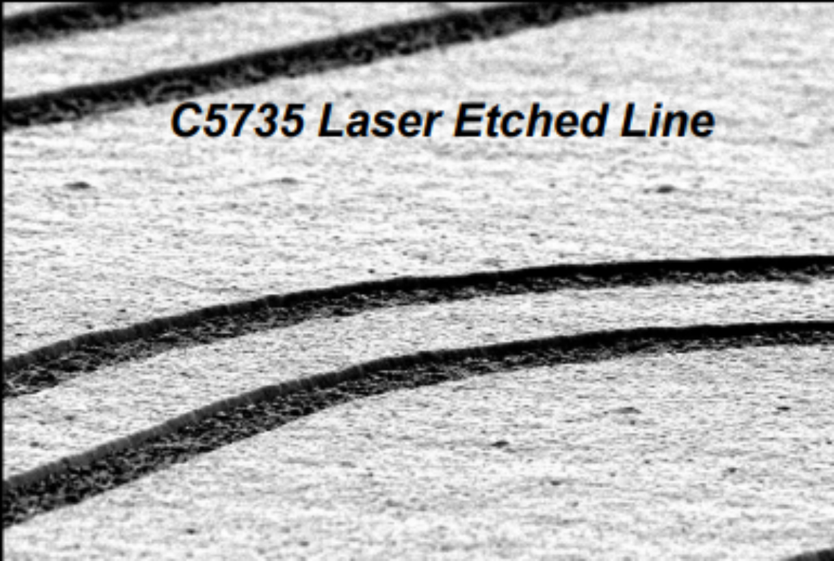
Instead, laser etching uses direct-write technology to etch patterns precisely where they’re needed quickly and cleanly. What once required multiple steps can now be completed in a single automated process.
For prototyping teams, this speed translates directly into innovation. Design iterations that once took days or weeks can now be executed in hours. For manufacturers, fewer process steps mean lower operational costs and greater consistency from part to part.
.png)
The benefits are immediate and measurable:
- Faster throughput through single-step processing
- Rapid design changes without retooling or new masks
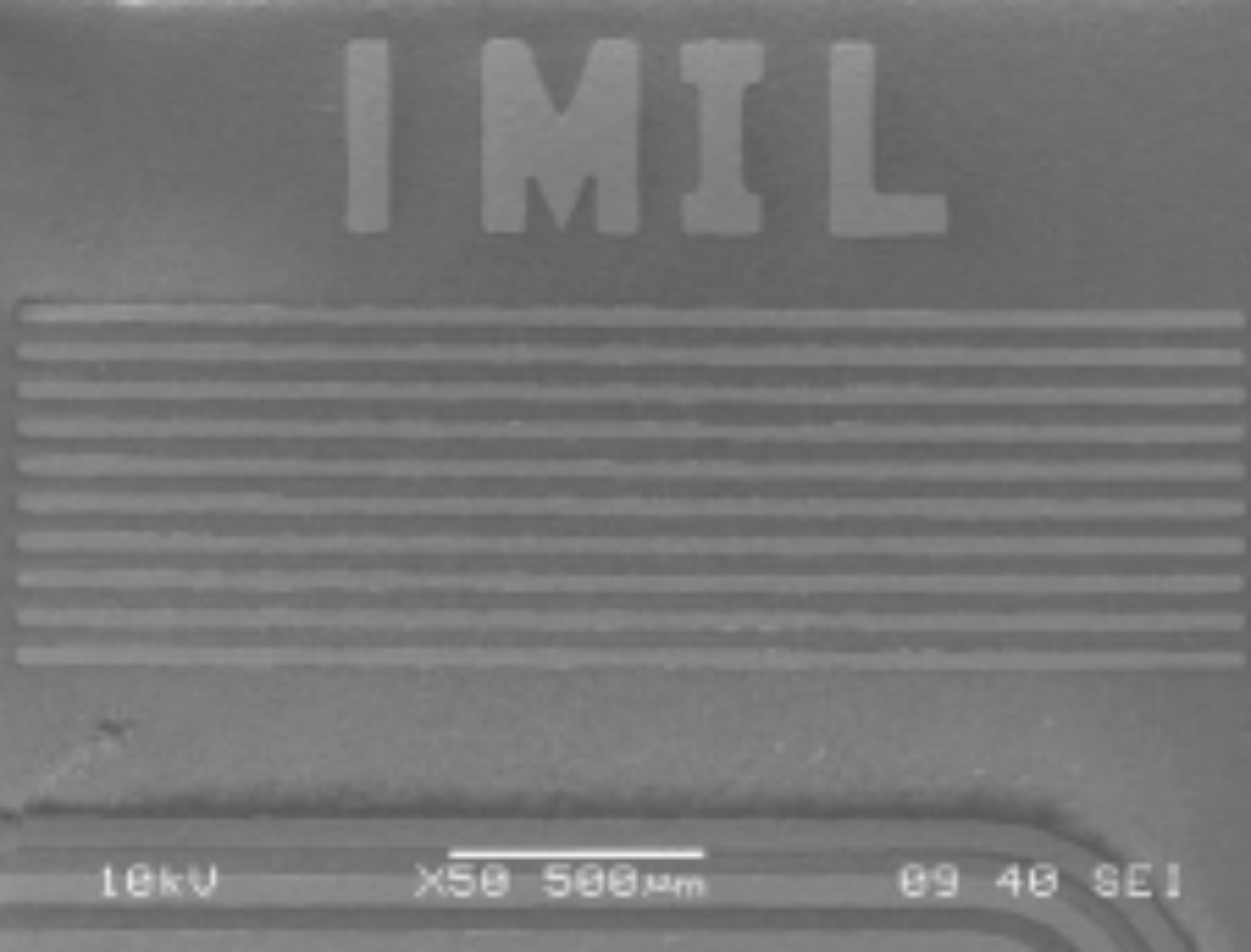
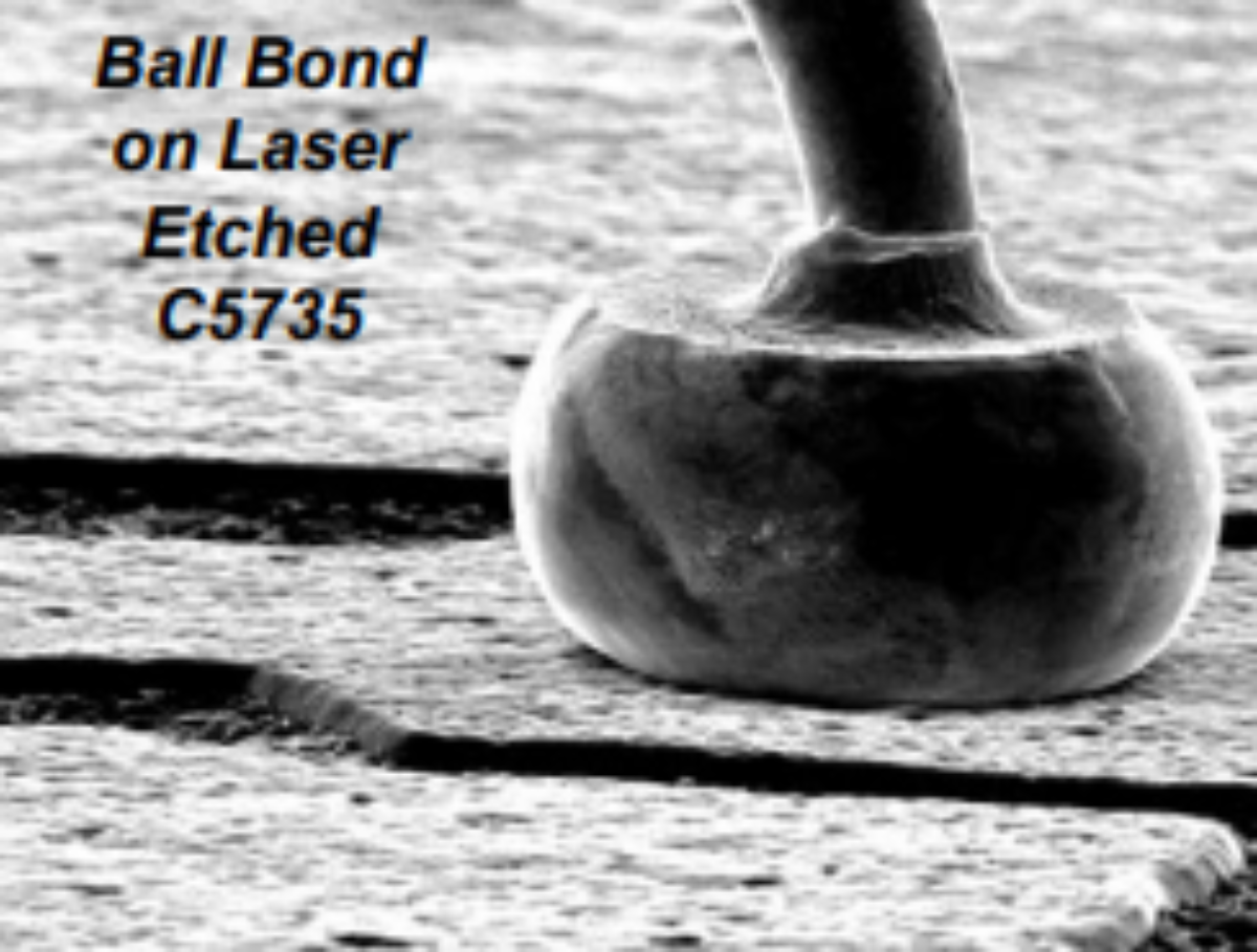
- Sharper line definition, achieving < 1 mil lines and spaces
- Reduced hazard management, minimizing chemical handling and safety overhead
Commercially available laser systems further expand what’s possible, offering flexible pulse rates and scanning speeds tailored to demanding RF applications.
.png)
The Bigger Picture: Manufacturing Built for What’s Next
As operating frequencies rise and RF systems continue to shrink, the manufacturing floor becomes just as important as the circuit design itself. Materials, metallization, and fabrication techniques must work together to meet tighter tolerances and shorter timelines.
Laser etching doesn’t just meet today’s demands. It anticipates tomorrow’s by streamlining workflows, reducing hazard reliance, and accelerating production, it allows manufacturers to focus less on managing processes and more on pushing technology forward.
Paired with thick-film gold metallizations such as C5735, which deliver corrosion resistance, dense microstructures, excellent electrical performance, and sharp line definition, laser etching provides a complete solution for demanding RF applications.
In a miniature world where precision is everything, laser etching isn’t just a tool, it’s a strategic advantage.